• Courses Images
M.Tech. in VLSI System Design

VISION: Be a pioneer in providing quality education in electronics, communication and allied engineering fields to serve as valuable resource for industry and society

Course Details


  • Course Duration : 2 Years
  • Intake : 24

About the Department


The Department of Electronics and Communication Engineering (ECE) was established in the year 2002-03, affiliated to Visvesvaraya Technological University (VTU), Belagavi and approved by All India Council for Technical Education (AICTE). The UG programme is accredited by the National Board of Accreditation (NBA), New Delhi till June 2025. The Department offer full-time UG programme in Electronics & Communication Engineering, PG programme in VLSI System Design and has a research centre recognized by VTU, Belagavi.

M.Tech (VLSI System Design) started in the year 2025-26, with an intake of 24 students. The Post Graduate Program in VLSI System Design is an affiliated program offered by Visvesvaraya Technological University (VTU), Belagavi. The autonomous curriculum is designed by team of experts in the VLSI domain.

Highly experienced faculty members with doctoral degrees handle the courses for this program. Faculty members are proactively involved in high end research activities and have published impetus research publications in domains of VLSI.


Why M.Tech. in VLSI System Design at BMSIT&M?


  • Industry-aligned Curriculum
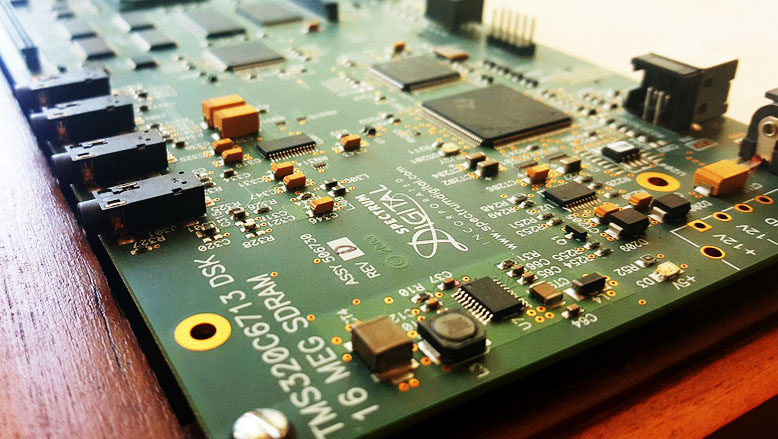
  • Access to EDA tools from Open POWER MicroWatt processor and build environment hosted on the PARAM Utkarsh Supercomputing Facility from CDAC and also C2S ChipIN program from CDAC
  • Partial course delivery by Industry experts
  • Industry Internships and Projects
  • Mentorship by top core Industry experts
  • Sponsored projects under DST,VGST etc.
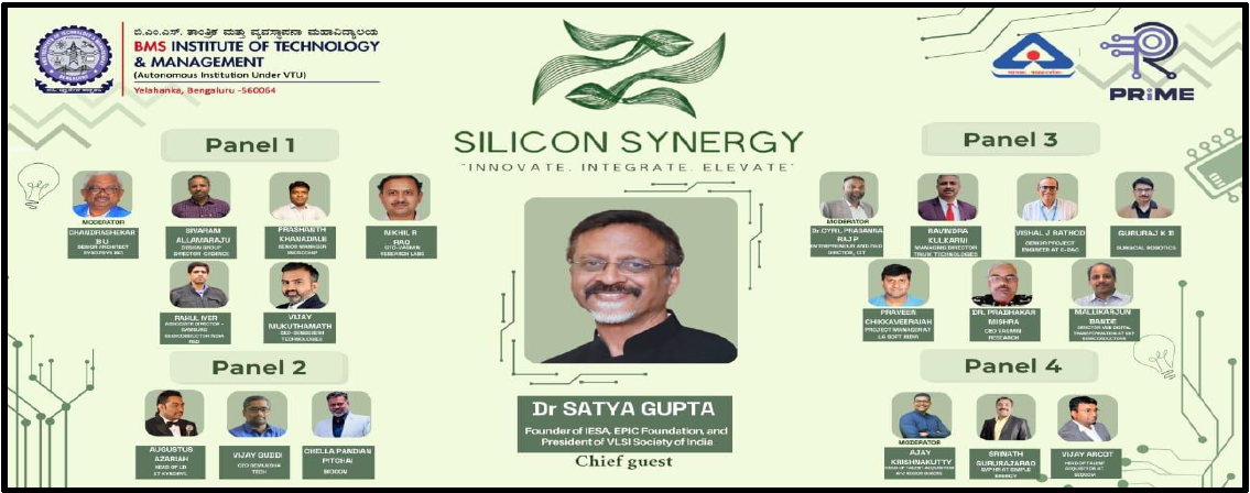

This makes graduates job-ready for VLSI related companies right after the completion.
Recent placement trends at BMSIT&M show increasing recruitment in core electronics companies and VLSI startups, with opportunities as:

  • VLSI Design Engineer
  • Verification Engineer
  • Physical Design Engineer
  • FPGA Design Engineer
  • ASIC Design and Testing Engineer

Sl. No Name Designation Role
1.       Dr. A Shobha Rani Professor and HOD,ECE, BMSIT&M Chairperson
2.         Dr. Banuprakash R Associate Professor & PG( VLSI System Design ) Coordinator Member
Two subject experts from outside the University nominated by the Academic Council
3.         Dr. Vinod Reddy Assistant Professor, IIITB, Bengaluru Member
4.         Dr. B P Harish Professor & Chairman, Dept.of ECE, UVCE, Bengaluru Member
VTU Nominee
5.         Dr. K V Suresh Professor & HoD,ECE SIT, Tumakuru Member
Two representatives from Industry relating to placements
6.         Mr.Sandeep Ganapathy Head ADAS & Autonomous driving, Tata Elxsi, Bengaluru. Member
7.         Dr. Sanjay Karambale Senior Manager, R&D division, Synopsys, Bengaluru. Member
Two representatives from Industry for M.Tech. VLSI System Design
8.         Mr. Mallikarjuna Bande Director, Design Enablement, AI-Driven Digital-Transformation. NXP Semiconductors, Bengaluru. Member
9.         Mr. Nikhil Rao Co-Founder, Chief Technologist, Vagmin Research Labs, Bengaluru. Member
One post-graduate meritorious alumnus
10.     Vinod G U Senior Engineer (SoC Engineer, VLSI), Qualcomm. Member
All the faculty members from Department of ECE

Be a pioneer in providing quality education in electronics, communication and allied engineering fields to serve as valuable resource for industry and society

1. To nurture students with a strong foundation in theoretical and practical concepts through innovative pedagogy and industry interface.

2. To foster interdisciplinary research, entrepreneurship skills and instill professional ethics by providing experiential learning opportunities.

  1. Excel in professional career, lead research in the area of VLSI and allied fields.
  2. Exhibit professional ethics, effective communication and teamwork in solving engineering problems by adapting industry standards for sustainable development of society.
  • PO1 : An ability to Apply the knowledge of Mathematics, Science and Engineering to solve VLSI Design problems
  • PO2 : An ability to Analyse and design complex VLSI circuits, using suitable analytical methods, Electronic Design Automation (EDA) tools.
  • PO3 : An ability to independently carry out research /investigation and development work to solve practical problems
  • PO4 : An ability to write and present a substantial technical report/document
  • PO5 : An ability to demonstrate a degree of mastery over the area as per the specialization of the program. The mastery should be at a level higher than the requirements in the appropriate bachelor program.

NEWSLETTERS